
UPenn ESE 3700 · Spring 2026
22nm CMOS Datapath & Memory
Transistor-level design of an 8-bit adder and a 16×4 SRAM (static random-access memory) array in the 22nm process provided by the course, covering the datapath and storage halves of any digital system. From Boolean derivation through Elmore delay modeling and SPICE (Simulation Program with Integrated Circuit Emphasis) validation. Projects from ESE 3700 at the University of Pennsylvania.
Project 1: 8-bit Ripple-Carry Adder
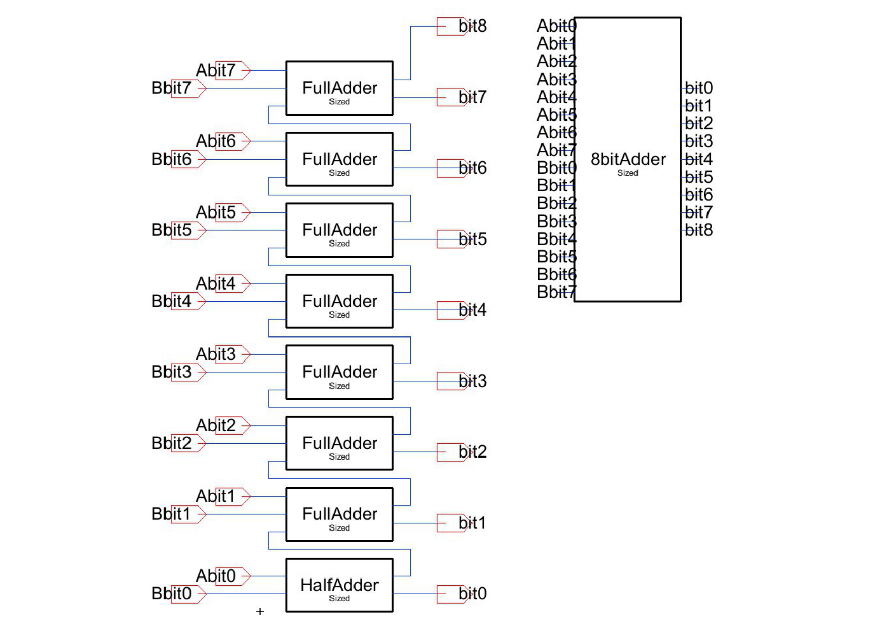
An 8-bit ripple-carry adder, built and simulated in Electric VLSI (very-large-scale integration). The complete datapath is eight bit-slices chained carry-to-carry: a half adder at bit 0 feeding seven full adders, each stage's Cout rippling up into the next stage's Cin.
Full Adder Bit-Slice
Each bit-slice is a full adder. Its two outputs are:
Both depend on A ⊕ B, which made XOR2 (a two-input exclusive-OR gate) the natural primitive to build around: compute it once, then feed it into both the sum and carry paths.
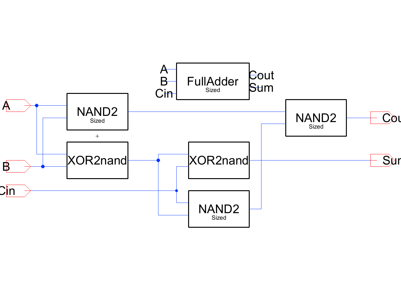
The full adder bit-slice combines the two primitives. One NAND2 (a two-input NAND gate) computes AB in parallel with the first XOR2 (P = A ⊕ B). That intermediate P feeds both the sum path (a second XOR2 producing S = P ⊕ Cin) and the carry path, where two right-hand NAND2 cells realize Cout = AB + Cin(A ⊕ B).
Sharing P between sum and carry is what makes this topology efficient: the most expensive intermediate is computed once and reused. Eight of these bit-slices are what make up the adder above.
XOR2 Implementation
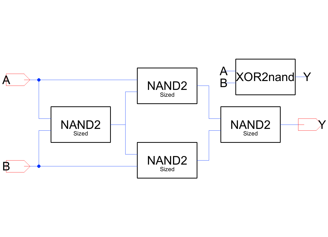
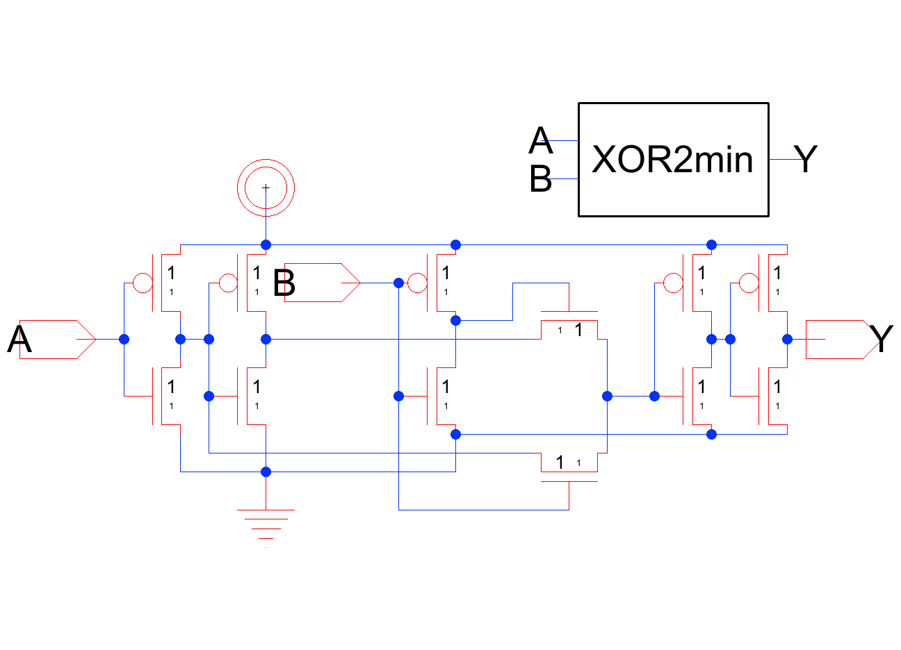
That bit-slice leans on an XOR2, so the last decision was which XOR2 to actually build it from. (Several alternative sum and carry topologies were explored and rejected along the way; that analysis is in the full report.) Two candidates were carried forward and compared head-to-head at the full 8-bit system level:
SPICE Results
Both designs were simulated across three transitions: an all-zeros to all-ones rising edge, the reverse falling edge, and a full carry ripple (255 + 1) that forces a carry to propagate through all eight bit-slices. That last case is the worst case for any ripple-carry adder, and it is the one that sets the maximum operating frequency.
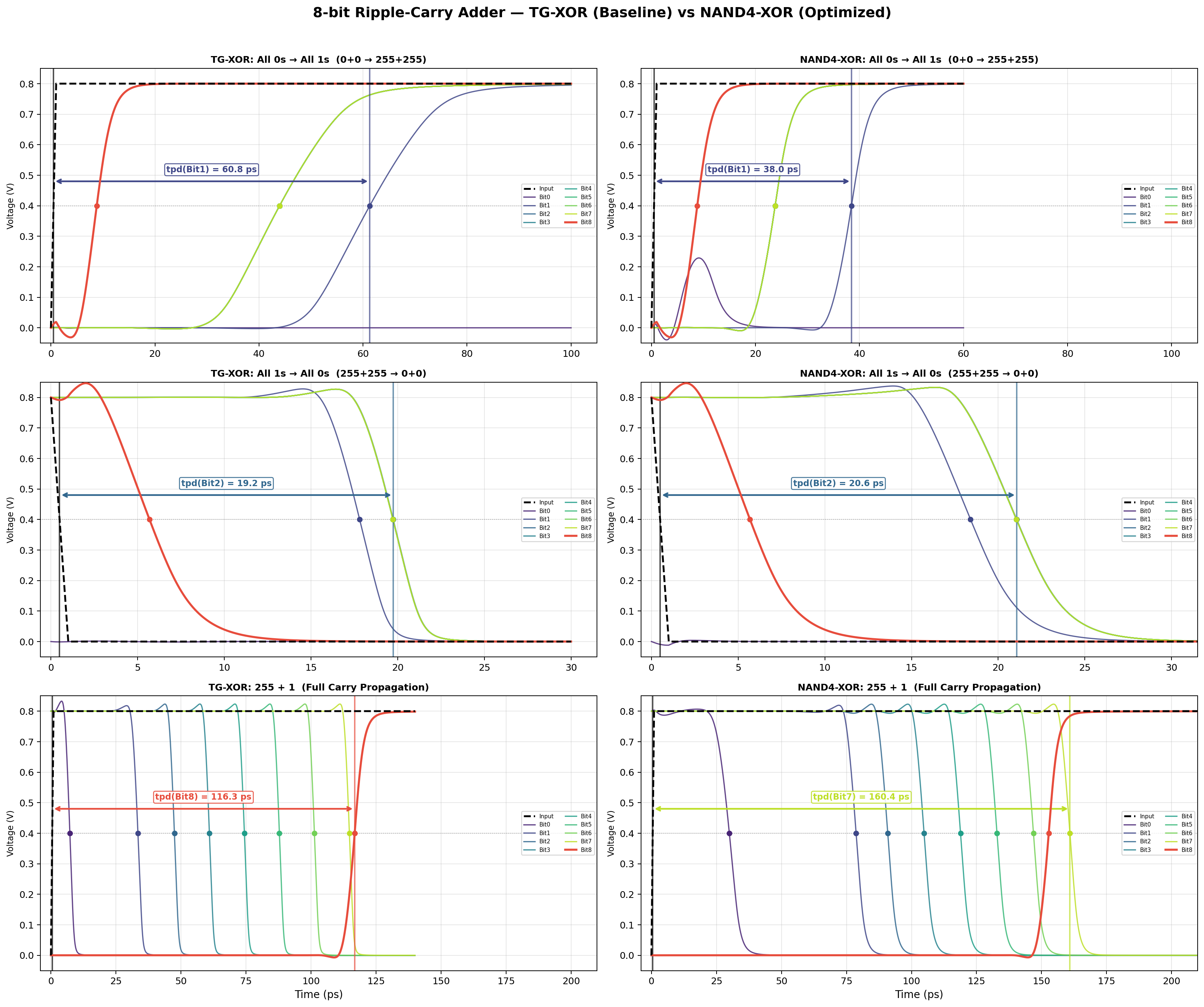
The two cells trade wins by transition type. On the rising edge the TG-XOR is actually slower, 60.8 ps against the baseline's 38.0 ps, because the transmission gate passes a weak high that the output buffer then has to restore. On the falling edge the two are within 1.4 ps of each other. The result that matters is the bottom row: on full carry propagation the TG-XOR settles in 116.3 ps versus the baseline's 160.4 ps, a 44.1 ps (27%) reduction. Because carry propagation sets the adder's maximum operating frequency, winning that worst case is what makes the optimized cell the better choice, even though it gives up ground on the non-critical rising transition.
Baseline Delay
160 ps
Optimized Delay
120 ps
Carry-Prop Speedup
−27%
Baseline Area
330 T
Optimized Area
240 T
Leakage Tradeoff
10×
The Lesson: When Elmore Lies
The most useful thing I learned on this project was not the topology exploration, it was what happens when your analytical model disagrees with simulation. Elmore delay predicted that widening the NAND2 PMOS (p-channel transistor) to 2×Wmin would cut pull-up delay roughly in half when driving the TG-XOR2 input. SPICE said the opposite: sizing up actually made carry propagation worse. The first-order RC (resistance-capacitance) model captures the resistance drop from a wider PMOS but not the extra capacitance added to internal nodes. I reverted to minimum-sized transistors everywhere. The numbers above come from that version.
The Leakage Tradeoff
The optimized design wins on delay and area, but transmission gates create a partially-conducting path from supply to ground at the worst-case input (A = B = 1). That's a ~10× leakage penalty vs. the fully static NAND-only baseline. At minimum-leakage inputs the two designs are comparable. The choice between them depends on duty cycle: high-throughput, mostly-switching paths want the optimized cell; always-on, low-activity datapaths want the baseline.
The full write-up covers the design-space exploration (sum options S1 through S4 and carry options C1 through C3), Elmore derivations with extracted capacitance and resistance values, all schematics, and the complete SPICE validation methodology.
Read the full report (PDF, 25 pages) →Project 2: 16×4 SRAM
A synchronous 16×4 SRAM (16 words of 4 bits) in the same 22nm process, targeting at least 500 MHz operation on a single clock input. The design spans the full memory system: a 6T (six-transistor) bit cell, non-overlapping clock generation, row and column decoders, sense amplifiers, column drivers, and a voltage midpoint reference. It is graded on a figure of merit that combines bitcell area, power, and delay squared, so every sub-block has to be sized for both correctness and score.
Top-Level Architecture
The full memory fits on a single schematic. Address inputs A0–A3 are latched and fed through a 4-to-16 row decoder gated by φ2, driving sixteen word-lines (WL) into the 16×4 bitcell array. Four column drivers precharge BL/BLb (the bit-line pair) during φ1 and drive writes during φ2; four isolated latch-type sense amps are armed by SAE (sense-amp enable), a delayed combination of φ2 and the write signal Wr, and resolve reads onto a per-column bus shared with the write path. A two-phase non-overlapping clock generator takes the single external clock (Clk) and produces the two phases that keep precharge and access strictly separated.
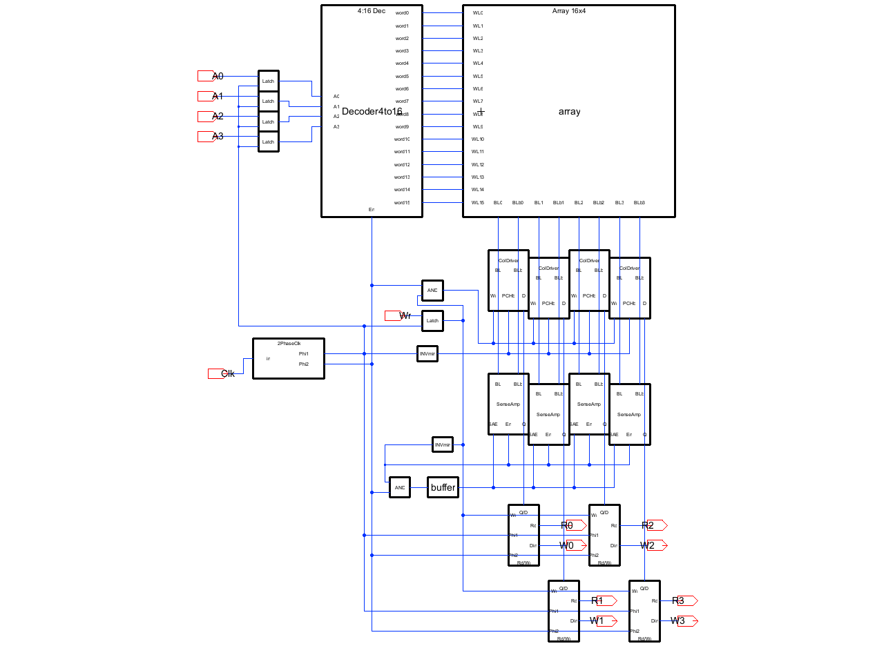
Two design decisions drive the rest of the implementation. First, PCHb is wired directly to φ1, which forces precharge to finish before φ2 can rise. The non-overlap gap is what guarantees the column drivers and word-lines never fight each other. Second, the sense amp is an isolated latch-type pair armed by a φ2-derived SAE, so it only fires once the bitline differential has developed past its offset. Every other block exists to feed these two.
6T Bitcell
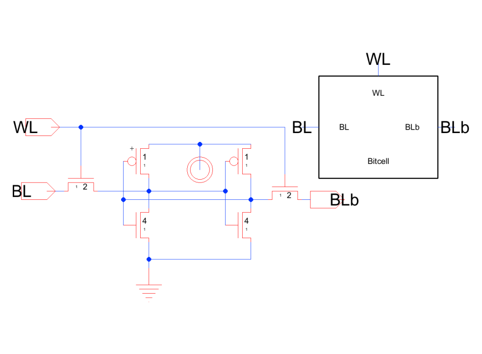
The whole array is sixteen by four of one cell. Two cross-coupled inverters hold the bit; two word-line-gated access transistors connect it to BL/BLb. The 4:2:1 PD:AX:PU (pull-down : access : pull-up) width ratio is what lets a read happen without flipping the stored value while a write can still overpower it. The report sizes and walks through every block built around it.
One Full Clock Cycle
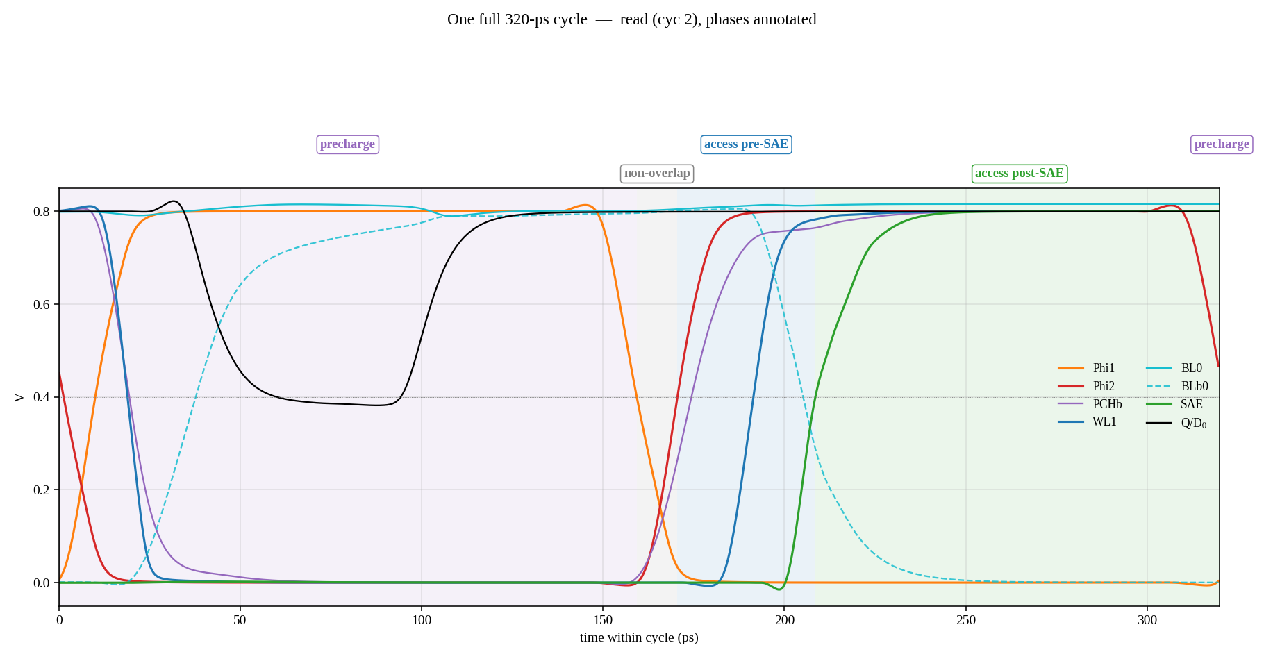
The easiest way to see the whole design work at once is to overlay every relevant signal on one clock period. I ran characterization at 320 ps (3.125 GHz), which is a deliberately safe choice: about 7% above the ~298 ps absolute minimum found by binary search further down, so no waveform is sitting right on its own failure boundary.
Functional Verification
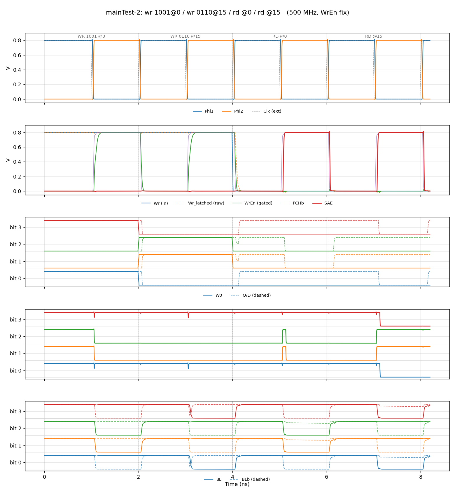
Correctness was validated bottom-up, from the bitcell up to the full array. The most interesting test is mainTest2: two different 4-bit words written to two different addresses, then read back. This checks that the decoder routes the correct row and that storing one word does not disturb another.
How Fast Can It Go?
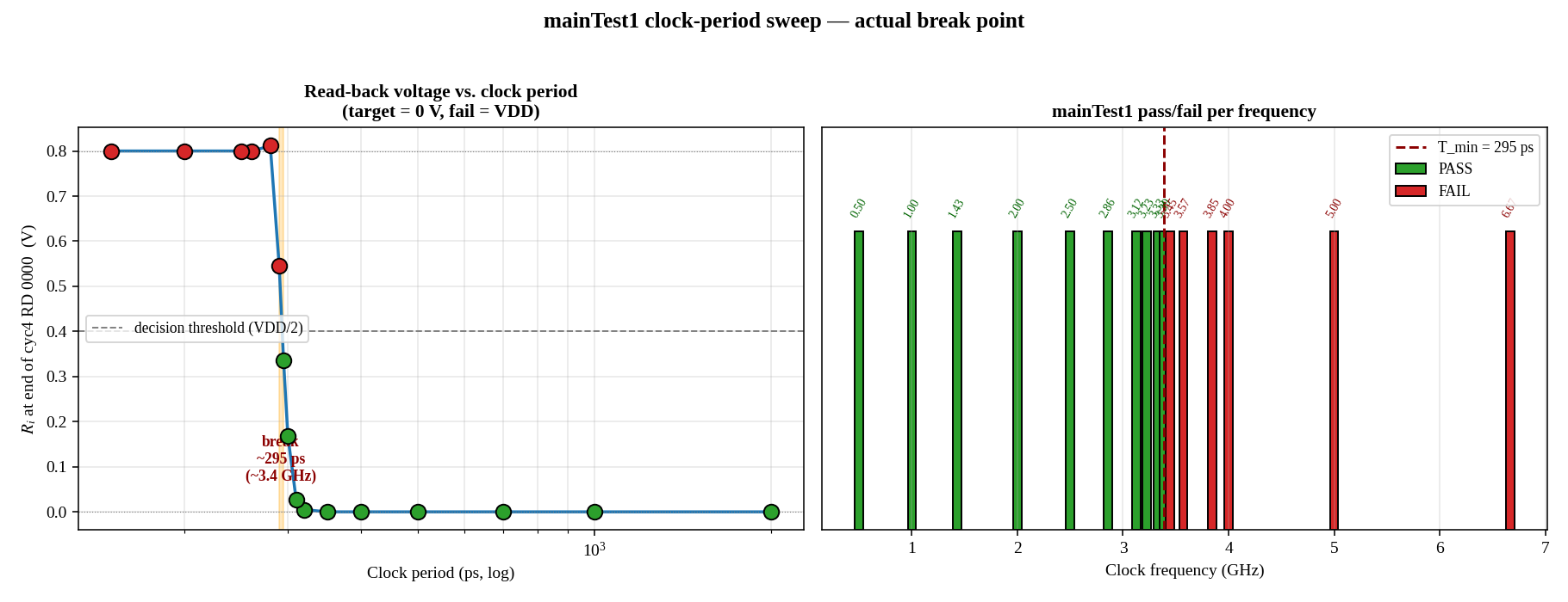
Minimum operating period was found with a binary search: shrink the clock period until reads stop matching the values that were written, then bracket the break point.
Where the Limit Is, and How I'd Push Past It
At Tmin the read path still finishes in roughly 92 ps. The write path is what gives out first. Looking back at the one-cycle plot, roughly half of every period is spent pulling BL and BLb back up to VDD during precharge. That long φ1 is what squeezes the access budget and pins Tmin where it is.
The immediate next step would be to upsize the precharge PMOS pair in the column driver (currently W = 2). A wider device pulls the bitlines up faster, shortens φ1, and redistributes the freed-up time to the access phase. That translates into a direct drop in Tmin without touching any of the more sensitive blocks. I didn't have time to sweep the PMOS width and re-run the search, but it's the one lever I'd pull first.
Summary of Metrics
This page is the highlight reel. The full report goes through every sub-block in detail: the 6T bitcell sizing, the two-phase clock circuit, the 4-to-16 decoder, the column driver, the isolated latch-type sense amp, the read/write input/output (I/O) block, the six timing invariants that guarantee correct operation, per-stage critical-path tables for both read and write, and the full figure-of-merit derivation.
Read the full report (PDF, 18 pages) →Both of these projects are finished for now, but it would be interesting to combine them: the 8-bit ripple-carry adder from Project 1 and the 16×4 SRAM from this project already cover the datapath and storage halves of a digital system, and wrapping them together with a small controller and a few logical operations would turn them into a simple arithmetic logic unit (ALU). A possible follow-on if I come back to this.